The Integrated Nanophotonics Group has been established at the University of Southampton department of Physics & Astronomy in 2009. Our research is aimed toward developing fundamental understanding and new applications of nanophotonics integrated in diverse fields ranging from silicon photonics to cell biology. Important elements of our work are plasmonic nanostructures, nanowires, and complex nanophotonic networks.
Plasmonic nanoantenna switches
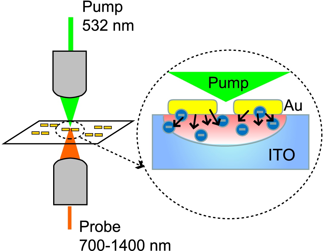
We have recently proposed a novel concept for switching of plasmonic nanoantennas using photoconductive gap loading. We are working to achieve nonlinear antenna switches experimentally. See this press release. We have introduced transparent conducting oxides including indium-tin oxide (ITO) and aluminium-doped zinc oxide (AZO) as novel plasmonic materials in the infared range. These materials have yet another interesting aspect, related to strong optical nonlinearity around the plasmon frequency (epsilon-near zero regime).
We have used plasmonic nanoantenna-metal oxide hybrids to achieve strong all-optical modulation. Starting from demonstration of picosecond, thermo-optic response, we proceeded to show hotspot-mediated ultrafast transfer of nonlinear modulation between closely spaced nanoantennas.
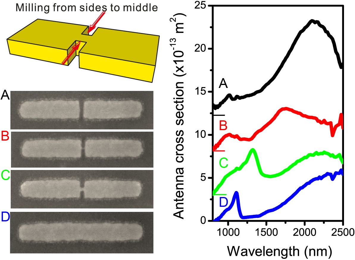
We are pushing the limits of nanofabrication and novel materials using the Southampton NanoCenter clean room facilities. Examples from our recent work include the use of helium-ion beam microscopy for milling of antenna nano-gaps with precision down to the nanometer-range. We have developed new quantitative optical spectroscopy of individual nanoantennas over a wide spectral range in the visible and near-infrared, which allows us follow the optical resonances and the transition from conductive to capacitive coupling regime as the antenna gap is precisely milled down.
Reconfigurable nanophotonic and plasmonic networks
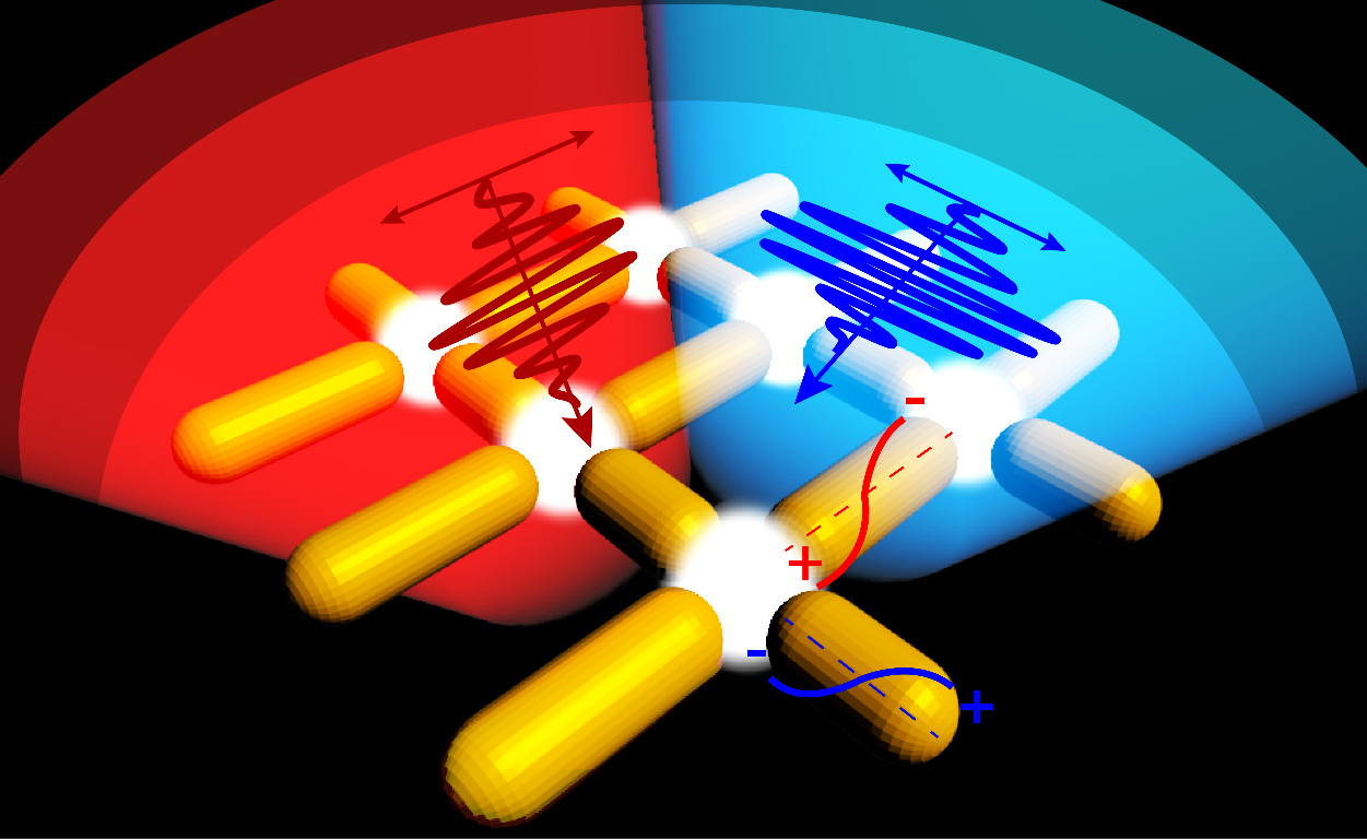
In 2012 Otto Muskens has been awarded a prestigious Early Career Fellowship by EPSRC to investigate and develop new types of nonlinear photonic devices inspired by fundamental concepts from mesoscopic physics. We have demonstrated ultrafast dephasing and reciprocity breaking in 3-D nanomaterials made from semiconductur nanowires. Recently, we have extended this work toward integrated photonic waveguides, where we are investigating ultrafast optical techniques for on-chip shaping of light in photonic integrated circuits.
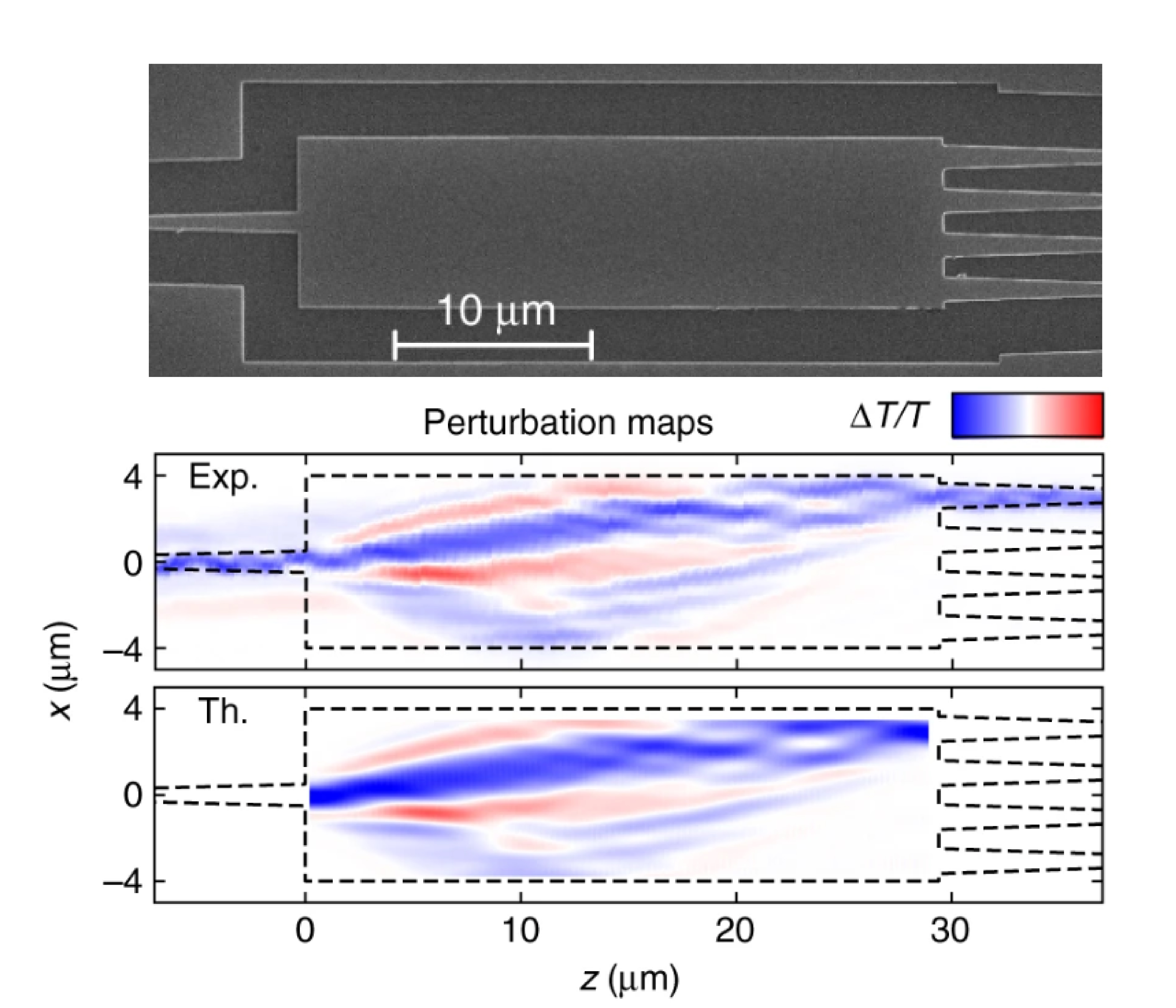
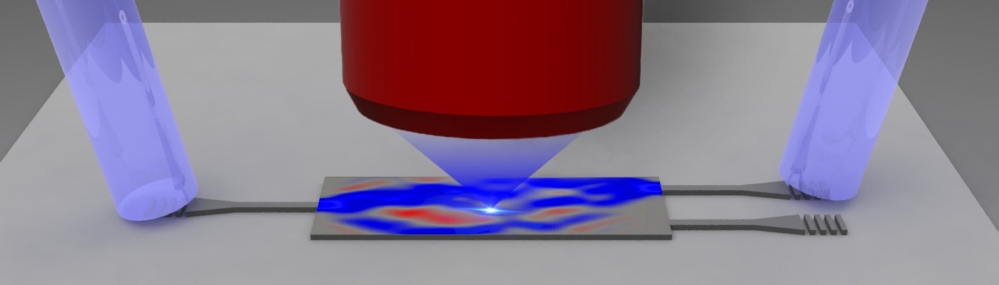
We have developed a new technique of Ultrafast Photomodulation Spectroscopy to characterise the flow of light in photonic chips. A perturbation is generated by a tightly focused uv laser beam from the top of the circuit, and its influence on telecom light travelling through the circuit is measured using a spectrometer. The technique simultaneously provides spectrally resolved information on the time of flight of light at any position and allows spatial mapping of the local sensitivity to perturbations yielding information on local fields and mode structure inside the waveguide. The method holds promise as a tool for testing of complex chips, complementary to methods such as near-field microscopy and afm-tip perturbation.
In recent work, we demonstrated all-optical control of light in silicon photonic devices using an integrated spatial light modulator. By controlling individual pixels on a multimode-interference device, we effectively routed light between the two outputs with 97% efficiency. This work opens up new avenues for developing reconfigurable devices, as explained in this press release.
Plasmonics & cells
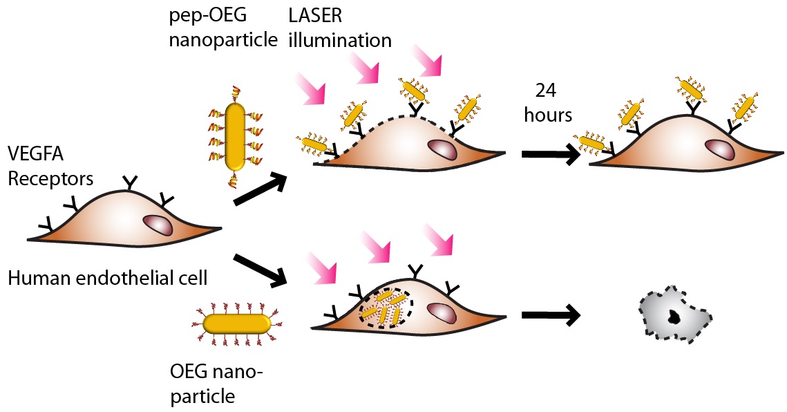
The use of nanotechnology in biomedine and healthcare is a rapidly expanding area of research. Specially engineered metal nanoparticles are employed in diagnosis and laser treatment, and as multifunctional vehicles for transporting biomolecules and targeting cells. In a collaboration with the Laboratory for Inorganic Nanocrystals of Antonio Kanaras, we aim at integration of ultrasensitive single-particle detection with real-time imaging in cells, as well as laser-induced treatment of different cell types using the plasmonic response of metal nanoparticles. We have demonstrated effective laser-induced treatment of human endothelial cells (HUVECs) exploiting the effective heat conversion of gold nanoparticles. Synergistic effects of nanoparticle heating and ligand functionality were identified, and were used to manipulate the process of in-vitro angiogenesis in co-cultures of HUVECs and cancer cells.
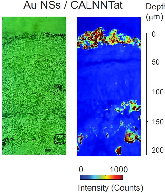
We are developing advanced spectroscopic techniques for detection of nanoparticles, including hyperspectral darkfield imaging and two-photon photoluminescence (TPPL). We use these techniques to characterise the distribution of nanoparticles in cells and in whole tissue samples such as skin.
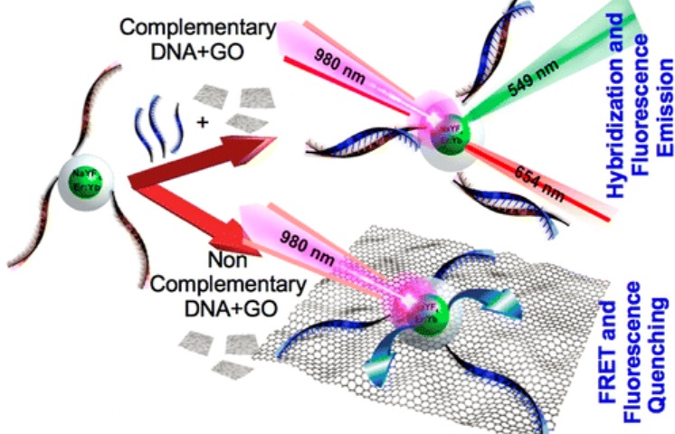
Next to the study of nanoparticle interactions with cells, inorganic nanoparticles functionalised with biomolecules such as DNA are used as sensitive detectors of specific sequences related to particular diseases. The Kanaras group is developing an ultrasensitive platform based on Er/Yb-upconversion nanoparticles and graphene oxide. Our first results are promising and show detection of specific DNA strands in the zeptomole range.
Light trapping and mesoscopic transport in nanowire materials
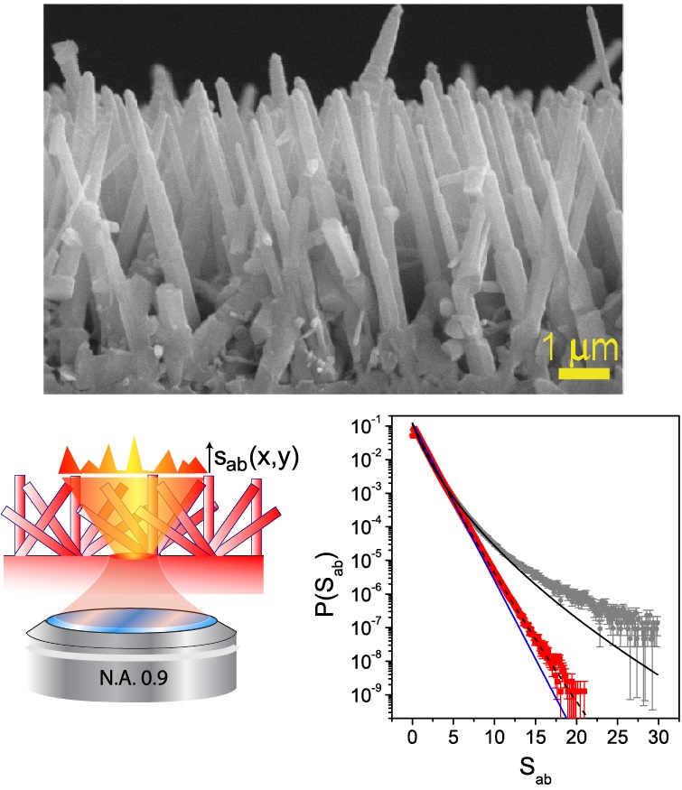
We have demonstrated that semiconductor nanowires form one of the strongest scattering materials for light available today. In our current experiments we extend our investigations to mesoscopic light transport and localization phenomena. It was shown that light transport is governed by only a few independent transmission degrees of freedom (channels), which results is strong correlations and fluctuations of the intensity distribution transmitted through a nanowire mat of several micrometers thickness. A popularized presentation of our work can be found here.
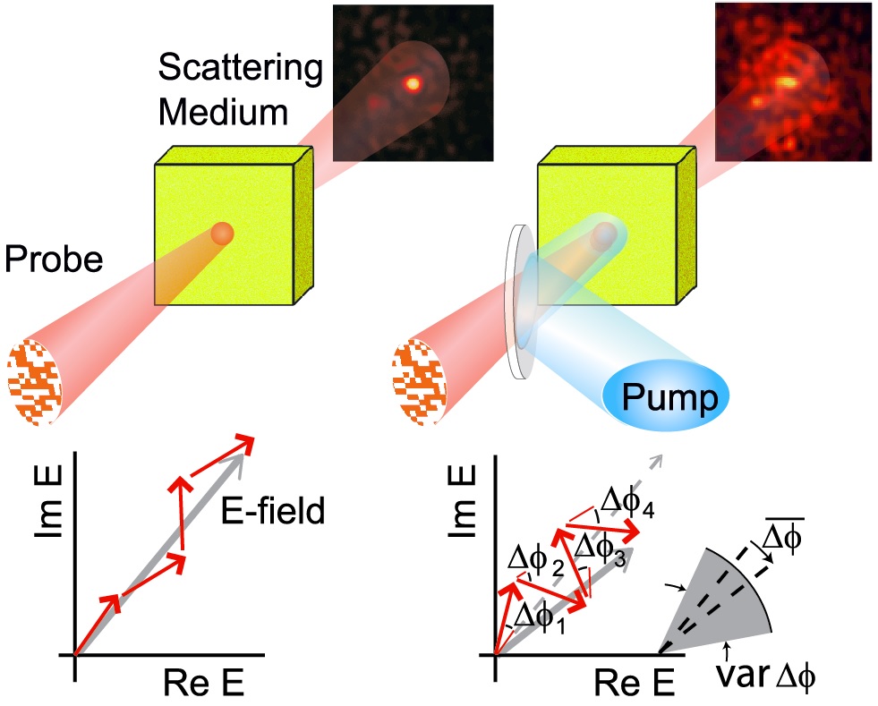
Next to strong light scattering, the semiconductor nanowires offer very strong optical nonlinearity when an ultrafast laser is used to photoexcite free carriers above the bandgap of the semiconductor material (548nm for GaP). We combine ultrafast control of transmission modes through nonlinear dephasing to control a shaped wavefront. Wavefront shaping using a spatial light modulator is used to concentrate light in a single bright speckle spot. Ultrafast pumping of the semiconductor produces a dephasing and corresponding suppression of the shaped light field. Next to suppressing coherent superposition state, it is also possible to increase the local intensity by optical pumping, through a revival of the shaped light field by nonlinear phase dynamics.